

2016-11-12
The use of delay lines to increase efficiency
I have to say that this article presents a hypothesis which at least has a good reason, but still requires the mandatory testing. The idea of the method is to separate the mutual influence of the two voltage sources through the delay line, and then adding power at its output.
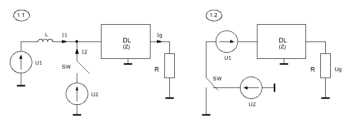
In figures (1.1) and (1.2) shows these two sources of voltage U1 and U2, the switch SW, the delay line DL and the active load — R. First, we describe the properties of elements U1, U2, DL, and then the operation of the circuit. The main requirement from sources U1 and U2 is small internal resistance. The delay line DL has an input impedance resistance, Z, is very small, the penetration resistance (we'll ignore that) and the time delay \(\tau\). The main feature of these circuits is the switching time, SW — it must be less than or equal to \(\tau\), and input impedance Z believe it is consistent with load: \(|Z| = R\).
The current method
Figure (1.1) presents the current method. Circuit DC U1-DL-R works indissoluble all the time, creating a current \(I_1\). Periodically, through the switch SW in the circuit is connected to source of U2; it creates an additional current \(I_2\). Since the source U1 is separated from the rest of the circuit the inductor L, the momentary connection of a source of U2, with a duration of less than or equal to \(\tau\), is not affected. The source U2 when connecting has only the input impedance of the delay line Z. after a time \(\tau\) at the load R appears a total current of \(I_g = I_1 + I_2\). This point we consider.
Since the voltage sources are independent, their required power during the period when the key SW is closed, are: \[P_1 = I_1^2\,R \qquad P_2 = I_2^2\,|Z| = I_2^2\,R \qquad (1)\] the power of \(P_1\) is independent of time and constant all over. Get on the load the power is: \[P_g = I_g^2\,R = (I_1 + I_2)^2\,R \qquad (2)\] Then comparing these capacities, we find the increment of efficiency of the second kind: \[K_{\eta2} = {P_g \over P_1 + P_2} = {(I_1 + I_2)^2 \over I_1^2 + I_2^2} \qquad (3)\] for Example, if \(I_1 = I_2\), then \(K_{\eta2} = 2\). Current method and will be considered in the experimental design below.
Method stress
This method is shown in figure (1.2). Unlike the previous sources U1 and U2 periodically for short periods of time \(\tau\) consistently. So all those calculations are already in tension: \[P_1 = U_1^2/R \qquad P_2 = U_2^2/|Z| = U_2^2/R \qquad (4)\] \[P_g = U_g^2/R = (U_1 + U_2)^2/R \qquad (5)\] \[K_{\eta2} = {P_g \over P_1 + P_2} = {(U_1 + U_2)^2 \over U_1^2 + U_2^2} \qquad (6)\] By analogy with the previous method, if \(U_1 = U_2\), then \(K_{\eta2} = 2\).
We must not forget that time period \(\tau\) may be small compared to the total period of \(T\), and hence the total increment of efficiency will be smaller than in (3), (6). This can be corrected, and even to increase these values if the source to make variables U1, with the frequency of the inverse \(T\), and a chain with a constant current of U1-DL-R to enter in a reactive mode. But this option is beyond the scope of this article, but here we consider the principle itself.
Delay line
The market offers quite a lot of industrial delay lines electrical impulses. But here we will consider a homemade DL that will help to reflect the principle of operation of schemes for (1.1) and (1.2). Let's start with the obvious — with a coaxial cable. All necessary parameters are given in tables, an example [1]. We only need to calculate the time delay \(\tau\) based on cable length and speed of propagation of waves in it. Also, you need to consider maximum power and voltage.
Less obvious variant is to use a symmetric long lines. Their calculation is more complex, but for homemade DL this option may be more appropriate [2].
And it is quite obvious solution would be to use as DL — inductors. In fact, it is necessary to make possible non-inductive, otherwise it will run as a regular high-pass filter that we here do not need. But since it's a coil, it is possible to merge it with the inductor L according to the scheme (1.1)? Here we discuss in more detail.
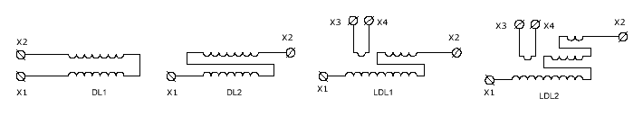
Coil to make a relatively non-inductive a variety of ways, but the simplest way to wind a single layer clockwise, then change direction, and the opposite side has to wind counterclockwise (DL1). But in this case the beginning and end of these layers will have a strong capacitive coupling and the short pulse can pass to the load bypassing the DL. You can go a different path and end-windings to spread in different directions of the coil (DL2). This option is much better, but we still don't solve the problem of combining DL and L from figure (1.1). This can be done, if part of the coil put on the choke, and the part under DL. Other slowly, part of the coil must be inductive, and the part is non-inductive. Short pulses of U2, in this case, we will need to apply for X3, X4 (LDL1). And to minimize capacitive coupling between input and output is possible, if a little to complicate the design and make non-inductive winding in the form of a pyramid (LDL2).

Considering all the previous calculations, it is now possible to make a diagram for the experiment. The diagram is not drawn, but in the inductive part of the coil can be inserted ferrite core to increase the inductance and, as a consequence, the decrease of mutual influence of sources of stress.
The calculation of such constructs is quite complex because in addition to the far non-linear properties of propagation of the waves in long lines, there is imposed a model of non-inductive coil. At the moment, such calculations do not exist, and yet dominated his Majesty — the experiment. The more experience and data for similar structures, the faster will the mathematical model for practical calculations.
The materials used
- [1] Coaxial cable
- [2] Feeder line